In semiconductor manufacturing, gasses do all the work, while lasers get all the attention. While lasers do etch transistor patterns into silicon, it is a range of gasses that deposit the silicon in the first place and resolve the etchings the laser made into a completed circuit. It should be no surprise that these gases, which are used to develop microprocessors through a multi-stage process, are high purity. In addition to that constraint, many of them have additional concerns and constraints. Some gasses are cryogenic, others corrosive, and others are extraordinarily poisonous.
Taken all together, these constraints make fabricating gas distribution systems for the semiconductor industry quite a challenge. Material specifications are demanding. In addition to the material specifications, the gas distribution array is a complex electro-mechanical array of interlinked systems. The environments in which they are being assembled are complex and overlapping. Final fabrication takes place in situ as part of the installation process. Orbital welding can help meet high-specification gas distribution requirements while simultaneously making fabrication in cramped challenging environments more manageable.
How Gases are Used in the Semiconductor Industry
It is necessary to understand at least the basics of semiconductor fabrication before attempting to plan for the fabrication of a gas distribution system. At its core, semiconductors are fabricated using gases to deposit near-elemental solids on a surface in a highly controlled manner. Then modifying those deposited solids by introducing additional gases, lasers, chemical etchants, and heat. Roughly the steps in the process are:
- Deposition: This is the process that creates the initial silicon wafer. A silicon precursor gas is pumped into a vacuum deposition chamber and, through either chemical or physical interactions, creates a thin silicon wafer.
- Photolithography: The photo part refers to a laser. At the higher extreme ultraviolet lithography (EUV) spectrum used to create the highest specification chips, a carbon dioxide laser is used to etch the circuitry of the microprocessor into the wafer.
- Etching: In the etching process, a halogen-carbon gas is pumped into the chamber, activated, and dissolves select materials in the silicon substrate. Effectively this process carves the circuit printed by the laser into the substrate.
- Doping: This is an additional step that modifies the conductivity of the etched surface to determine the exact conditions under which the semiconductors are conductive.
- Annealing: In this process, a reaction between layers of the wafer is initiated by elevating pressures and temperatures. Essentially it finalizes the results of the previous process and creates the final completed processors in the wafer.
- Chamber and Line Cleaning: The gases used in the previous steps, especially etching and doping, are frequently highly toxic and reactive. So process chambers and the gas lines that feed them need to be filled with a neutralizing gas that reduces or eliminates harmful reactivity and then an inert gas that prevents intrusion of any contaminating gases from the external environment.
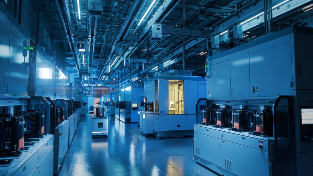
Gas distribution systems in the semiconductor industry tend to be complicated due to the fact there are so many different gases involved, and the control exercised over the flow of the gas, its temperature, and its pressure over time must be so exacting. This is further complicated by the ultra-high purity needed for each gas in the process. The gas used in the previous step must be flushed out of the lines and chambers or otherwise neutralized before the next process can begin. This means that there are significant numbers of dedicated lines, interfaces between welded tube systems and hoses, interfaces between hoses and tubes and gas regulators and sensors, and interfaces between all of the previously mentioned components and valve and seal systems designed to prevent line contamination when gas supplies are swapped out.
Additionally, there will be bulk gas supply systems external to clean rooms and specialty gas both within clean room environments and specialized containment areas to mitigate any hazards in case of an accidental release. Welding these gas systems in such a complicated environment is not an easy task. However, with care, attention to detail, and the right equipment, the task can and is successfully done.
Fabricating Gas Distribution Systems in the Semiconductor Industry
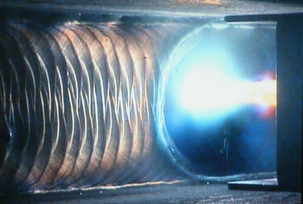
The materials used in semiconductor gas distribution systems can be highly variable. They can include things like metal tubes and hoses lined with Teflon to resist highly corrosive gases. The most commonly used material for general-purpose tubing in the semiconductor industry is 316L stainless steel—a low-carbon stainless steel variant. When it comes to 316L vs. 316, it is 316L that is more resistant to intergranular corrosion. An important consideration when dealing with a range of highly reactive and potentially volatile gases that can erode carbon. When welding 316L stainless steel, fewer carbon precipitates are released. It also reduces the potential for grain boundary attack, which can cause pitting along the weld line and the heat-affected zone.
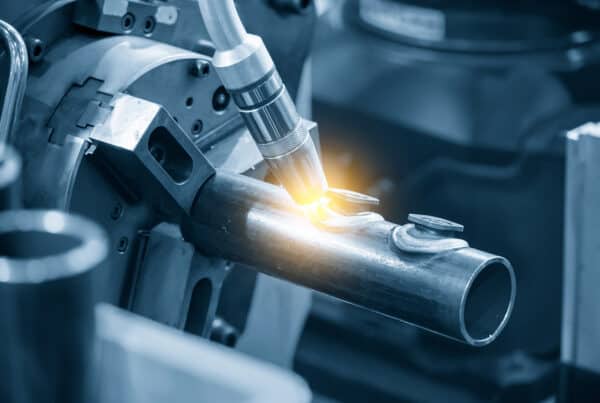
To reduce the potential for corrosion and contamination of product lines resulting from pipe corrosion, 316L stainless steel welded using pure argon shielding gas and gas tungsten arc welding (GTAW) orbital welding is the standard for the semiconductor industry. GTAW is the only welding process that provides the control needed to maintain a high-purity environment in the process pipe. Automated orbital welding simply provides the repeatable process control required to complete welds during the fabrication of gas distribution systems for semiconductors. The fact that closed orbital weld heads can fit in the crowded and difficult spaces found in the complex interchanges between process areas is also a significant advantage for the process.
However, semiconductor fabs are complex, and there are a wide variety of different interfaces. Successfully completing welding on all these different interfaces requires a range of orbital TIG welding parameters. Fortunately, modern tube welding power supplies can be programmed with a complete range of qualified parameters that have been found to meet the required specifications. This greatly simplifies production gas distribution systems for semiconductor fabs and related industries.
Arc Machines Inc. has decades of experience providing orbital welding equipment to the semiconductor industry for welding the 316L stainless steel tubing that’s standard in semiconductor fabs and expertise in developing welding parameters to meet high gas.